



The rain that had lashed the site all morning had eased by the time the speeches began, and by early afternoon a mild September sun was working its way across the yard outside the former Bosch and Johanna Solar halls in Brandenburg an der Havel. Guests from the Bundestag, the city administration, the local technical university, the State Ministry of Economic Affairs and investors had assembled under a marquee to hear David Ward, chief executive of Oxford PV, thank the teams in Oxford and Brandenburg for a decade of, as he put it, proving that "a technology born in the laboratory could become a viable industrial reality".
The company acquired the site in 2016, when it employed around thirty people in the United Kingdom and was still, as chairman Christian Langen recalled, "constantly preparing the next financing round". Buying a full-scale factory from Bosch was, on paper, reckless. The counter-arguments, Langen told the audience, were all correct: too big, too early, too risky. Oxford PV did it anyway. One of Langen's sharper memories from the early months is driving into town to buy an internet router at the local Media Markt, because Bosch had switched the line off and the new occupants had inherited a factory without a connection.
The smarter E – perovskites are a long time coming
Ten years on, the site employs more than a hundred people and hosts what Oxford PV describes as the world's first integrated production line for perovskite-silicon tandem cells and modules. Sonja Eichwede, SPD member of the Bundestag for the region, told the audience that hearing "Oxford" and "Brandenburg an der Havel" in the same sentence still made her heart beat a little faster. Mayor Daniel Keip was more direct: Oxford PV's technology, he said, had effectively saved a plant that had already lived through the collapses of Bosch Solar and Johanna Solar.
Inside the line
The tour that followed, led by chief technology officer Ed Crossland, made clear how tightly the company has fused conventional heterojunction manufacturing with its own perovskite know-how. The underlying architecture is straightforward in principle: a crystalline silicon heterojunction cell, coated with amorphous silicon, serves as the bottom substrate, with a temperature-sensitive perovskite layer deposited as a thin film directly on top. The two absorbers capture different parts of the solar spectrum, pushing efficiency well beyond the roughly 25 percent practical ceiling of single-junction silicon.
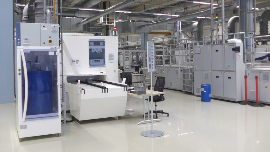
The tour continued into the perovskite rooms, where photography was no longer permitted. In the silicon hall behind them, standard European and Asian tools texture, clean and coat 100 to 150 micrometre wafers with amorphous silicon in vacuum chambers a few tens of atoms thick. The equipment mix reflects that pragmatism: European suppliers, among them Berlin-based Jonas & Redmann, sit alongside Asian tool makers, with raw materials such as silicon sourced globally. The perovskite rooms, Crossland added drily, are where the "secret sauce" sits.
Hans-Christoph Neidlein
Physically, the perovskite tools look much like their silicon counterparts: a tray of wafers enters one end, a thin film is deposited, the tray emerges at the other. The difference is temperature. Perovskite cannot tolerate the heat used in standard silicon processing, so several tools have been lengthened to run cooler and slower while achieving the same result.
A new wafer tray enters each tool approximately every minute, with all equipment and processes operating at or above 1,000 wafers per hour throughput, supporting a heterojunction bottom cell production nameplate capacity of around 100 MW, while the integrated tandem line has nameplate capacity in the tens of megawatts under continuous four-shift operation. In practice, the factory operates two shifts, splitting its time between commercial production for customers and development campaigns for new recipes and materials.
Crossland was candid about the site's role. Brandenburg exists to prove that the process works at commercial performance levels and is manufacturable. Individual tools here handle throughputs an order of magnitude below what a modern heterojunction gigafactory would use, but the per-wafer process time is already representative. "Once we demonstrate through our line that it works, you have confidence to buy the bigger tool," he said. The finished cells then join a familiar module assembly flow, stringed with conductive adhesive and laminated into standard glass-glass formats that are visually almost indistinguishable from conventional silicon panels.
Product, roadmap and scale-up
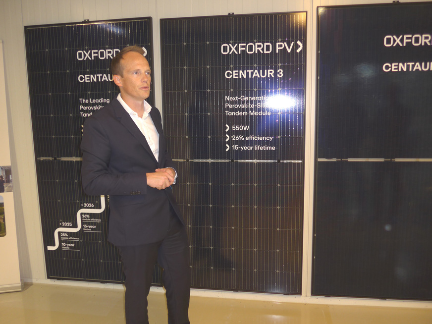
The current commercial module is a bifacial glass-glass panel of around 25 percent efficiency. A generation-three product, the Centaur 3, is scheduled for market release in 2026, rated at 550 W with 26 percent efficiency and a 15-year warranty. A further step is planned for 2027, targeting a 20-year warranty and 27 percent efficiency. The internal roadmap, according to Laura Miranda, chief strategy officer of Oxford PV, has held to a consistent rhythm of roughly one percentage point of efficiency gain per year, with 35 percent module efficiency in view by 2035 and an ambition to undercut the levelised cost of silicon-only technology by around 20 percent by 2035.
Hans-Christoph Neidlein
Alongside the mainstream product, the company is expanding a specialty line for lightweight and flexible applications, including modules for high-altitude aircraft wings and stratospheric communications platforms, where efficiency per unit area and per unit mass is decisive. A shingled tandem concept module, first shown at Intersolar Europe in Munich, hints at further module-level gains by eliminating ribbon interconnections and reclaiming inactive area. Oxford PV also holds what Miranda describes as the largest intellectual property portfolio in the perovskite field, a position the company sees as central to its long-term commercial strategy.
Expert view – how perovskite can overcome durability concerns
Demand, Miranda said frankly, already exceeds what Brandenburg can supply. Oxford PV wants to scale to gigawatt-level manufacturing, though not at the current site. Whether the next factory lands in Germany, elsewhere in the European Union or further afield remains open, and the company is actively weighing its options. Research and development funding has supported the technology to date, and although EU support for European manufacturing has so far been out of reach for a company of its size, Oxford PV is engaging with policymakers as the conversation around European industrial capacity gathers pace. Licensing agreements for use of Oxford PV's IP in mainstream solar applications, with Trina Solar for sales in China and with First Solar for sales in the United States, extend the reach of the technology into two of the world's largest solar markets.
Perovskite – Oxford PV and Trinasolar sign patent agreement
Looking ahead
Back under the marquee, as staff and guests queued for ice cream and a food truck fired up for the evening, the atmosphere was one of quiet confidence. Ten years in, Oxford PV has done what few in the solar industry believed possible in 2015: moved perovskite-silicon tandems from the laboratory into a working factory, secured customers on three continents and set out a credible pathway to gigawatt-scale manufacturing. Ward closed the afternoon by noting that the first decade had been about proving perovskite-silicon tandems could reach commercial status. The next, he suggested, will be about how far the technology can travel. (hcn)