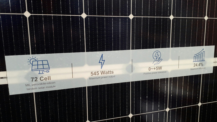
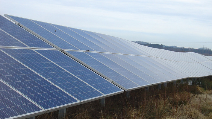
In this week's Topic of the Week we are looking at some of the up-and-coming trends in solar energy. A hot subject matter – one that we will also come back to later in the week – is perovskite solar cells:
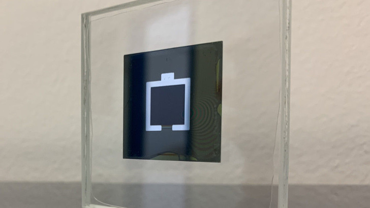
Researchers at the Helmholtz Centre Berlin (HZB) have increased the record efficiency of perovskite solar cells to 29.15 percent. They achieve this efficiency with a crystalline solar cell on which an additional semiconductor layer of perovskite is applied. This is a hybrid compound of inorganic and organic substances. The advantage: While silicon primarily uses the red parts of sunlight to produce electricity, the perovskites also process the blue parts of the light spectrum.
Layers optimized
With this new record, confirmed by Fraunhofer ISE, the Berliners are close to their goal of breaking the 30 per cent efficiency threshold. Ideas for further increasing efficiency are already on the table. The degree of efficiency has also been confirmed by the American National Renewable Energy Laboratory (NREL). It is the result of international cooperation. "We developed a special new contact layer for the record cell in cooperation with the group of Vytautas Getautis from Kaunas University of Technology and optimized another intermediate layer," explain Eike Köhnen and Amran Al-Ashouri, who were involved in the further development on the part of HZB.
Special silicon cell used
This new contact layer made it possible to further adapt the composition of the perovskite compound so that it is more stable in the tandem solar cell under illumination and contributes even better to the electricity balance. The researchers also used a special silicon cell. This is because the lower cell was provided with an additional composite layer of silicon oxide before the researchers applied the perovskite layer. This is used for the optical coupling of the two individual cells.
Scaling up is possible
As with all printed semiconductor technologies, the challenge now is scaling up from laboratory scale to module scale. However, the researchers do not see any problem here. After all, the first attempts at production using vacuum processes have been successful. (mfo)
Here, in case you missed it, is Part 1 of last week's series on BIPV.


